Measured on hardware
Results beyond simulation
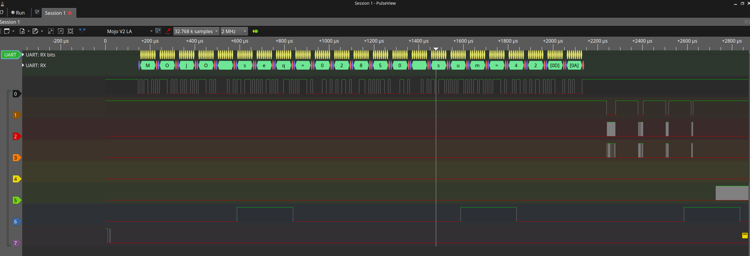
I validated captures using a NUCLEO-L476RG generating known signals. UART at 115200 baud decoded correctly at 2 MS/s; SPI at 1.25, 2.5, 5, and 10 MHz decoded at 50 MS/s; and the 1 MHz timer signal measured a 1000 ns period at 100 MS/s. A 65,536-sample counter capture had zero sequence breaks across rates from 2 to 100 MS/s.
Sparse-signal run-length compression captured approximately 1.10 seconds at 2 MS/s—about 34× the raw uncompressed window for that test signal. This is workload-dependent, not a guaranteed improvement for dense traffic.
Implementation
Capture hardware with an existing software frontend
The FPGA samples eight digital inputs into block RAM, with up to 65,536 raw samples, and implements up to four sequential value-and-mask trigger stages. Run-length compression extends captures for signals with long idle periods. A SUMP-compatible interface lets PulseView handle acquisition control, visualization, and protocol decoding.
Engineering tradeoffs
Throughput and timing constraints
The fixed 500 kbaud microcontroller-to-host serial link sustains approximately 45.5 KB/s, so a full capture takes around 1.6 seconds to download; this is capture-then-transfer, not live streaming. The top advertised PulseView sampling option exceeds the FPGA design’s actual 100 MS/s maximum. The repository documents these limits, compressed-mode trigger-marker limitations, and a board serial-port handling quirk addressed by the launch script.
FPGA utilization reached 17% of LUTs and 23% of slices while using all 32 block RAMs, with 100 MHz timing met on the documented build.
Verification
Repeatable tests and an external signal source
The repository includes an Icarus Verilog simulation workflow, reusable bench test code, STM32-based waveform generation, FPGA build scripts for Xilinx ISE, and host-side load/launch utilities. These separate logic verification from end-to-end measurements made on the real Mojo and STM32 boards.
Next iteration · not yet built
Protected inputs and deeper captures
I’m exploring an expansion shield with 1.8–5 V input-level support, overvoltage protection, additional channels, PSRAM capture storage, and a faster FT232H-based readout. The shield is currently an architecture and bench-simulation effort: no schematic, PCB, or shield hardware has been completed or validated yet.